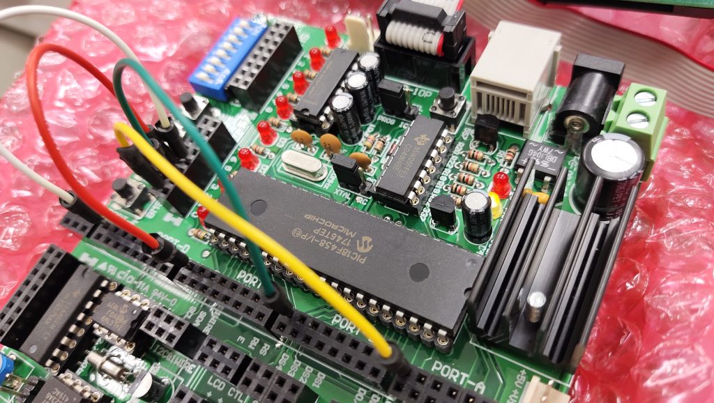
After creating the project and basic programming code from the previous article using MPLAB X IDE, this article is the use of a microcontroller to be used as a signal output unit or Output and input signal or Input through the port of PIC18F458 both port A, B, C and D through circuit LED and Switch.
GPIO
GPIO or General Purpose Input/Output is a pin of the microcontroller that can be used to operate as signal input, signal output part, or special functions such as a pin for PWM, counter, waiting for an interrupt or for reading/exporting analog signals, etc.
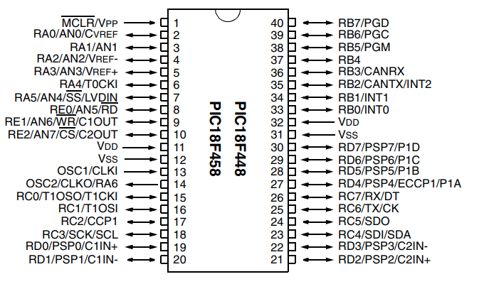
From the pin layout of the PIC18F458 microcontroller in Figure 2, it can be seen that several pins are both Input/Output and some pins are only input or output. In addition, some pins have more than one function, for example, pin 40 is either Input/Output pin acts as RB7 or input/output port B 8th (bit 7) and can perform PGD functions. Also, pin 37 acts as both an input and an output, but only acts as the 5th bit (bit 4) of port B, etc.
from : p.4 of PIC18F458 Datasheet
From Figure 3, the microcontroller has ports A, B, C, D and E called PORTA, PORTB, PORTC, PORTD and PORTE. The pins of these ports are GPIO and the names of each pin are as follows.
- RA0,RA1,RA2,RA3,RA4,RA5 and RA6, 7 pins of port A
- RB0, RB1, RB2, RB3, RB4, RB5, RB6 and RB7, 8 pins of port B
- RC0, RC1, RC2, RC3, RC4, RC5, RC6 and RC7, 8 pins of port C
- RD0, RD1, RD2, RD3, RD4, RD5, RD6 and RD7, 8 pins of port D
- RE0, RE1 and RE2, 3 pins of port E
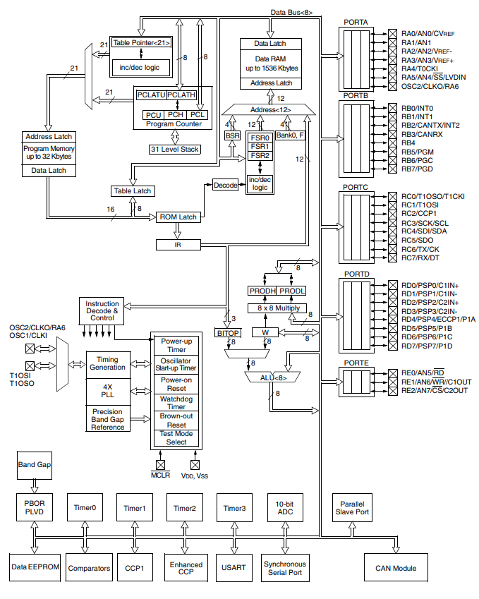
From : p.11, Figure 1-2: PIC18F448/458 Block Diagram
Directional controlling
Ports A, B, C, D, and E can be assigned the direction of operation to be the input or output pin with the configuration in the following registers.
- TRISA for assigning pins duty of port A
- TRISB for assigning pins duty of port B
- TRISC for assigning pins duty of port C
- TRISD for assigning pins duty of port D
- TRISE for assigning pins duty of port E
Determine which pin is an input signal, an output signal must give the value of that pin 0, and if it wants to be an input signal, set the value of bit or pin as 1.
- 1, if input
- 0, if output
Accessibility
There are two ways to configure/read pins or access pins on each port: specify the sequence of
pins as follows:
- For port A i.e. RA0, RA1, RA2, RA3, RA4, RA5 and RA6
- For port B i.e. RB0, RB1, RB2, RB3, RB4, RB5, RB6 and RB7
- For port C i.e. RC0, RC1, RC2, RC3, RC4, RC5, RC6 and RC7
- For port D i.e. RD0, RD1, RD2, RD3, RD4, RD5, RD6 and RD7
- For port E i.e. RE0, RE1 and RE2
or refer to the port name as follows
- PORTA represents port A
- PORTB represents port B
- PORTC represents port C
- PORTD represents port D
- PORTE represents port E
The output to a pin or port has the following form: 1 means it sends a level 1 voltage in the digital signal to that pin, and 0 means that the pin is Ground. In the case of sending data to port B, it will be an integer without +/- symbols.
name = 1
name = 0
port = 8 bits
And the case of reading from a pin or port has the following format:
pin = name
port = name
I/O Ciruit
Circuits for import and export have different working principles:
- The import will read the value from the state that appears at the moment.
- The signal output must consider the circuit that receives the signal from the microcontroller how much voltage and current are needed.
- If the microcontroller can drive voltage and current directly, connect the pin of the microcontroller to the output circuit. This direct drive voltage and current are called Source Current or a microcontroller as a power supply for an external circuit.
- In the case that the microcontroller does not have enough current to drive the external circuit, design an external circuit to work when the pin of the microcontroller is 0 or GND is called Sunk Current.
Examples of import and export circuits that are used as circuits on the lab board are switches and LEDs.
LED circuit
The digital signal output circuit of the experimental board is a circuit that works as Source Current, which is to drive current from the pin of the microcontroller because PIC18F458 can drive a lot of current and the circuit that is an LED does not require much current to work, so it does not need to be designed to work like a sink current.
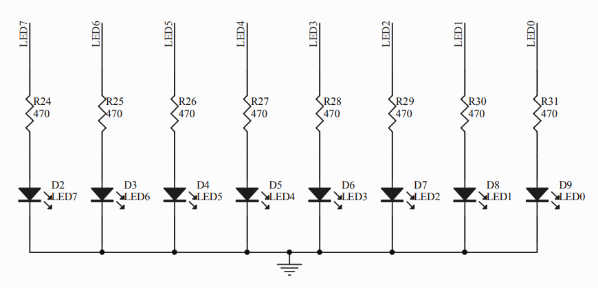
From Figure 4, it can be seen that one side of the LED pin is connected to a resistor that is directly connected to the microcontroller pin and connected to the GND of the system, therefore, when transmitting digital signal 1, the circuit is complete, resulting in a bright LED lamp On the other hand, when sending 0, there is no voltage flowing through the LED, thus causing the LED to not light.
Switch circuit
A switch is a type of input device used in computer systems. There are 5 switches on the test board which are 1 dip switch (blue body and white lever) and 4 push button switches.
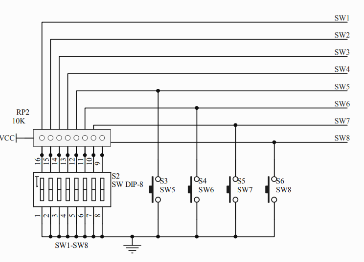
From Figure 5, it can be seen that S2 or SW DIP-8 which is the switch of the dip switch is connected to pin SW1, SW2, SW3, SW4, SW5, SW6, SW7 and SW8. The push-button switches S3, S4, S5 and S6 are connected to SW5, SW6, SW7 and SW8.
When considering the circuit, it can be seen that power is connected to the pin on one side of the switch and it is the same side that is connected to the microcontroller input pin. The other side of the switch is connected to the GND of the system, so
- If SW DIP-8, or S3, S4, S5, S6 is a closed circuit (or push the switch) will cause the voltage to flow from the power supply to GND quickly, so there is no voltage to the pin of the microcontroller. As a result, the voltage value is received as a digital signal 0.
- If the switch state is open or not pressed, there is the voltage on the microcontroller pin, so the voltage reading at the pin is digital signal 1.
Example Code
from the principle of controlling the direction of the port, port access, and an example of an LED and a switch circuit when applied to write a program for a guideline as follows
Blink the LED from RA0, RB0, RC0, RD0
The first example is to connect pins RA0, RB0, RC0 and RD0 to an LED circuit at lamps 0, 1, 2 and 3. All ports A, B, C and D must be OUTPUT with the following command.
To send voltage to the pin use the following command.
To change the state of the pin to GND so that the lamp is turned off as follows:
And the delay must set the speed of XTal to 20MHz and set the OSC to HS and the delay command is __delay_ms( number of milliseconds ).
// CONFIG1H
#pragma config OSC = HS
#pragma config OSCS = ON
#pragma config PWRT = OFF
#pragma config BOR = ON
#pragma config BORV = 25
#pragma config WDT = OFF
#pragma config WDTPS = 128
#pragma config STVR = ON
#pragma config LVP = ON
#pragma config CP0 = OFF
#pragma config CP1 = OFF
#pragma config CP2 = OFF
#pragma config CP3 = OFF
#pragma config CPB = OFF
#pragma config CPD = OFF
#pragma config WRT0 = OFF
#pragma config WRT1 = OFF
#pragma config WRT2 = OFF
#pragma config WRT3 = OFF
#pragma config WRTC = OFF
#pragma config WRTB = OFF
#pragma config WRTD = OFF
#pragma config EBTR0 = OFF
#pragma config EBTR1 = OFF
#pragma config EBTR2 = OFF
#pragma config EBTR3 = OFF
#pragma config EBTRB = OFF

#include <xc.h>

#define _XTAL_FREQ 20000000

void main(void) {

    TRISA = 0x00;
    TRISB = 0x00;
    TRISC = 0x00;
    TRISD = 0x00;

    while (1) {
        RA0 = 1;  // LED ON
        RB0 = 1;  // LED ON
        RC0 = 1;  // LED ON
        RD0 = 1;  // LED ON
        __delay_ms(500); // 1 Second Delay
        RA0 = 0;  // LED OFF
        RB0 = 0;  // LED OFF
        RC0 = 0;  // LED OFF
        RD0 = 0;  // LED OFF
        __delay_ms(500); // 1 Second Delay
    }
    return;
}
Running LED with PORTC
This example takes all C ports as OUTPUT pins and initializes them to 000000012 or 0x01, after which bits are shifted to the left. After moving to position 100000002 or 0x80, revert to 0x01 again and keep repeating
// CONFIG1H
#pragma config OSC = HS
#pragma config OSCS = ON
#pragma config PWRT = OFF
#pragma config BOR = ON
#pragma config BORV = 25
#pragma config WDT = OFF
#pragma config WDTPS = 128
#pragma config STVR = ON
#pragma config LVP = ON
#pragma config CP0 = OFF
#pragma config CP1 = OFF
#pragma config CP2 = OFF
#pragma config CP3 = OFF
#pragma config CPB = OFF
#pragma config CPD = OFF
#pragma config WRT0 = OFF
#pragma config WRT1 = OFF
#pragma config WRT2 = OFF
#pragma config WRT3 = OFF
#pragma config WRTC = OFF
#pragma config WRTB = OFF
#pragma config WRTD = OFF
#pragma config EBTR0 = OFF
#pragma config EBTR1 = OFF
#pragma config EBTR2 = OFF
#pragma config EBTR3 = OFF
#pragma config EBTRB = OFF

#include <xc.h>

#define _XTAL_FREQ 20000000

void main(void) {
    unsigned char patt = 0x01;
    TRISC = 0x00;
    while (1) {
        PORTC = patt;
        __delay_ms(100);
        patt <<= 1;
        if (patt == 0) {
            patt = 0x01;
        }
    }
    return;
}
Press buttun on, off
This example uses port C with 4 bits for OUTPUT and 4 bits for INPUT.
- RC0 connected to SW5
- RC1 connected to SW3
- RC2 connected to SW7
- RC3 connected to SW8
- RC4 connected to LED0
- RC5 connected to LED1
- RC6 connected to LED2
- RC7 connected to LED3
This causes the value of TRISC to be set to 0x0F or 000011112. The working relationship is as follows.
- Subtract RC0 with 1 and send to RC4
- Subtract RC1 with 1 and send to RC5
- Subtract RC2 with 1 and send to RC6
- Subtract RC3 with 1 and send to RC7
// CONFIG1H
#pragma config OSC = HS
#pragma config OSCS = ON
#pragma config PWRT = OFF
#pragma config BOR = ON
#pragma config BORV = 25
#pragma config WDT = OFF
#pragma config WDTPS = 128
#pragma config STVR = ON
#pragma config LVP = ON
#pragma config CP0 = OFF
#pragma config CP1 = OFF
#pragma config CP2 = OFF
#pragma config CP3 = OFF
#pragma config CPB = OFF
#pragma config CPD = OFF
#pragma config WRT0 = OFF
#pragma config WRT1 = OFF
#pragma config WRT2 = OFF
#pragma config WRT3 = OFF
#pragma config WRTC = OFF
#pragma config WRTB = OFF
#pragma config WRTD = OFF
#pragma config EBTR0 = OFF
#pragma config EBTR1 = OFF
#pragma config EBTR2 = OFF
#pragma config EBTR3 = OFF
#pragma config EBTRB = OFF

#include <xc.h>

#define _XTAL_FREQ 20000000

void main(void) {
    TRISC = 0x0F;
    while (1) {
        RC4 = 1-RC0;
        RC5 = 1-RC1;
        RC6 = 1-RC2;
        RC7 = 1-RC3;
        __delay_ms(100);
    }
    return;
}
Conclusion
From this article, the reader has learned the steps of port orientation, port access, port pin access and apply the principle to the circuit of the LED and Switch sector on the course experimental board which is the basis for further application such as changing from the LED circuit to the relay circuit for turning on and off the light or solenoid to turn off the water, etc. Finally, have fun with programming.
(C) 2022, By Anuchart Boonmark, Jarut Busarathid and Danai Jedsadathitikul
Updated 2022-03-22