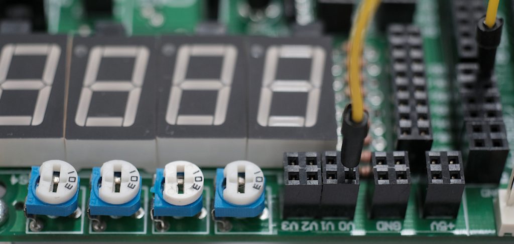
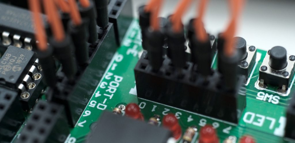
This article uses the GPIO of the PIC18F458 microcontroller connected to an ADC module or an analog-to-digital converter module for reading voltage levels in the 0 to 5V range from the input signal. This allows the system designer to consider the details of the voltage from the circuit, such as from the variable resistor, resistors change their values according to the brightness or microphone values, for example, to process these values or enter the next working condition, such as reading the voltage to report the result as a voltage in the Lo, Hi or unstable level, etc. On the computer architecture experiment board, there are 4 sets of adjustable resistor circuits as shown in Figure 1 makes it possible to study programming to use the ADC module and be able to apply it in the future.
ADC
ADC or Analog-to-Digital Converter is a method of converting input from an analog signal into a digital number. The resulting numerical value is within the range of resolution from the codec module. The PIC18F458 microcontroller has a conversion resolution of 10 bits, or 210, which allows it to convert the input voltage readings in the 0V to 5V range to 0 to 1023 or 1024 numerical values.
Analog signal input
There are 8 input pins named AN0, AN1, AN2, AN3, NA4, AN5, AN6, and AN7, distributed in ports A and E as follows:
- RA0 is AN0
- RA1 is AN1
- RA2 is AN2
- RA3 is AN3
- RA5 is AN4
- RE0 is AN5
- RE1 is AN6
- RE2 is AN7
The working diagram of the module is shown in Figure 2.
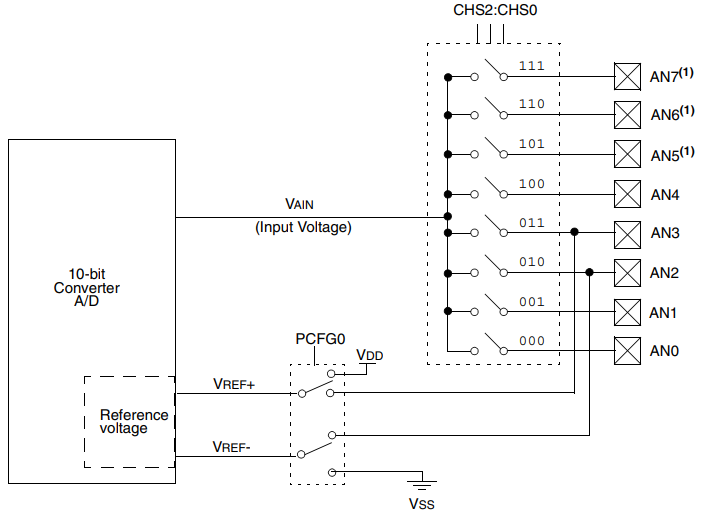
From Figure 20-1 A/D BLOCK DIAGRAM p.243 of PIC18F458 Datasheet of Microchop (2006)
ADC Sector Control
The operation of the ADC module is controlled by registers ADCON0 and ADCON1, readings are placed in ADRESH and ADRESL registers to store the byte and low byte of the read value all of which are 8-bits.
ADCON0
The ADCON0 register is located in the microcontroller’s RAM at position 0xFC2. The value of each bit of the register is as follows.
| bit 7 | bit 6 | bit 5 | bit 4 | bit 3 | bit 2 | bit 1 | bit 0 |
| ADCS1 | ADCS0 | CHS2 | CHS1 | CHS0 | GO/DONE’ | – | ADON |
When the microcontroller is started or reset it has a value of 0000 00-0, but if an interrupt from the WDT (Watch Dog Timer is a timer for the software side to send a signal to the timer to know if the software is working properly. This is for verifying whether the software hangs or not and if it hangs it will reset itself) and return to working in the program. The value of this register is not changed.
ADCON1
The ADCON1 register is located at the microcontroller’s RAM at position 0xFC1 and has the details of each bit as follows.
| bit 7 | bit 6 | bit 5 | bit 4 | bit 3 | bit 2 | bit 1 | bit 0 |
| ADFM | ADCS2 | – | – | PCFG3 | PCFG2 | PCFG1 | PCFG0 |
The initial state of ADCON1 when started or reset is 00== 0000 and after verification of WDT, the set value remains the same as it was set before the WDT was executed.
The meaning of the settings in the ADCON0 and ADCON1 registers is as follows.
- The frequency of operation of the converter module is determined from the values of ADCS2, ADCS1 and ADCS0 according to Table ep6-3.
| ADCON1.ADCS2 | ADCON0.ADCS1 | ADCON0.ADCS0 | Meaning |
| 0 | 0 | 0 | FOSC/2 |
| 0 | 0 | 1 | FOSC/8 |
| 0 | 1 | 0 | FOSC/32 |
| 0 | 1 | 1 | FRC |
| 1 | 0 | 0 | FOSC/4 |
| 1 | 0 | 1 | FOSC/16 |
| 1 | 1 | 0 | FOSC/64 |
| 1 | 1 | 1 | FRC |
- The channel selection that is being set up is defined with CHS0, CHS1 and CHS2 in ADCON0 as in Table ep6-4.
| CHS2 | CHS1 | CHS0 | Meaning |
| 0 | 0 | 0 | select AN0 |
| 0 | 0 | 1 | select AN1 |
| 0 | 1 | 0 | select AN2 |
| 0 | 1 | 1 | select AN3 |
| 1 | 0 | 0 | select AN4 |
| 1 | 0 | 1 | select AN5 |
| 1 | 1 | 0 | select AN6 |
| 1 | 1 | 1 | select AN7 |
- To activate the ABC of the specified channel, set the ADON bit where
- 0 means stop the operation
- 1 means start or continue the operation
- To check whether the codec has finished working or not. This can be checked by the GO/DONE bit, where 0 means the job is done, 1 means the codec module is working.
- Determining the format of the bit-sorting of the resulting results is done by assigning values to ADFM as shown in Figure 3.
- 1 means that it is Right Justified, it stores values from right to left, i.e. bits 9,8,7,6,5,4,3,2,1 and 0. Bits 0 to 7 are stored in ADRESL and 8 to 9. Store in bits 0 and 1 of ADRESH.
- 0 means it is Left Justified to store from left to right, or sequence bits 0,1,2,3,4,5,6,7,8 and 9 cause bits 0 to 7 stored in ADRESH. Bit 8 and 9 are stored in bits 7 and 6 of ADRESL.
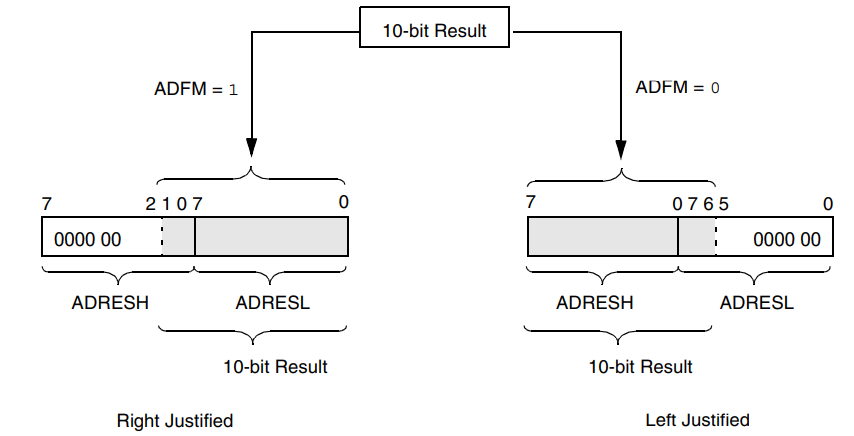
From Figure 20-3 A/D RESULT JUSTIFIED p.247จ ofPIC18F458 Datasheet of Microchop (2006)
- Determining the modes of the pins in making ADC is determined from bits PCFG3, PCFG2, PCFG1 and PCFG0, giving values according to Table ep6-5 and their meanings are as follows:
- A means working as an analog signal input
- D means working as a digital signal input
- VREF+ Means it works as a reference voltage input REF+.
- VREF- Means it works as a reference voltage input REF-
- VDD Means the reference voltage applied to the VDD pin is applied.
- VSS Refers to the reference voltage applied to the VSS pin.
- C/R It is the number of pins that are analog inputs and the number of pins that are used as voltage inputs for reference.
| PCFG | AN7 | AN6 | AN5 | AN4 | AN3 | AN2 | AN1 | AN0 | VREF+ | VREF- | C/R |
| 0000 | A | A | A | A | A | A | A | A | VDD | VSS | 8/0 |
| 0001 | A | A | A | A | VREF+ | A | A | A | AN3 | VSS | 7/1 |
| 0010 | D | D | D | A | A | A | A | A | VDD | VSS | 5/0 |
| 0011 | D | D | D | A | VREF+ | A | A | A | AN3 | VSS | 4/1 |
| 0100 | D | D | D | D | A | D | A | A | VDD | VSS | 3/0 |
| 0101 | D | D | D | D | VREF+ | D | A | A | AN3 | VSS | 2/1 |
| 0110 | D | D | D | D | D | D | D | D | – | – | 0/0 |
| 0111 | D | D | D | D | D | D | D | D | – | – | 0/0 |
| 1000 | A | A | A | A | VREF+ | VREF- | A | A | AN3 | AN2 | 6/2 |
| 1001 | D | D | A | A | A | A | A | A | VDD | VSS | 6/0 |
| 1010 | D | D | A | A | VREF+ | A | A | A | AN3 | VSS | 5/1 |
| 1011 | D | D | A | A | VREF+ | VREF- | A | A | AN3 | AN2 | 4/2 |
| 1100 | D | D | D | A | VREF+ | VREF- | A | A | AN3 | AN2 | 3/2 |
| 1101 | D | D | D | D | VREF+ | VREF- | A | A | AN3 | AN2 | 2/2 |
| 1110 | D | D | D | D | D | D | D | A | VDD | VSS | 1/0 |
| 1111 | D | D | D | D | VREF+ | VREF- | D | A | AN3 | AN2 | 1/2 |
So
- The TRISA or TRISE function of the channel to be input analog signal must be set to 1.
- The operation settings must be set in the ADCON0 and ADCON1 registers.
- The result of transcoding is stored in ADRESH and ADRESL registers according to the format defined in ADFM bits.
Example Code
An example program of this article is to read the values from the adjustable resistor on the test board connected to AN0 or pin RA0 as shown in Figure 4. After that, convert the values to be divided into 9 levels for display. At the 8 LED bulbs connected to port D as shown in Figure 5, each level has the effect as follows.
- Level 0 from 0 to 112 mean led 0, 1, 2, 3, 4, 5, 6 and 7 off
- Level 1 from 113 to 225 mean led 0 on
- Level 2 from 226 to 338 mean led 0, and 1 on
- Level 3 from 339 to 451 mean led 0, 1 and 2 on
- Level 4 from 452 to 564 mean led 0, 1, 2 and 3 on
- Level 5 from 565 to 677 mean led 0, 1, 2, 3 and 4 on
- Level 6 from 678 to 790 mean led 0, 1, 2, 3, 4 and 5 on
- Level 7 from 791 to 903 mean led 0, 1, 2, 3, 4, 5 and 6 on
- Level 8 from 904 to 1023 mean led 0, 1, 2, 3, 4, 5, 6 and 7 on
Settings for ADCON0 and ADCON1 to enable AN0 to work, with the other pins being digital as usual. and collecting data in a Right Justified manner, thus doing the following:
- setting for ADCON0 are
- ADCS1, ADCS0 เป็น 0 กับ 0
- CHS2, CHS1, CHS0 เป็น 0, 0 และ 0
- for ADCON1 are
- ADFM is 1
- ADCS2 is 0
- PCFG3, PCFG2, PCFG1, PCFG0 is 1,1,1 and 0
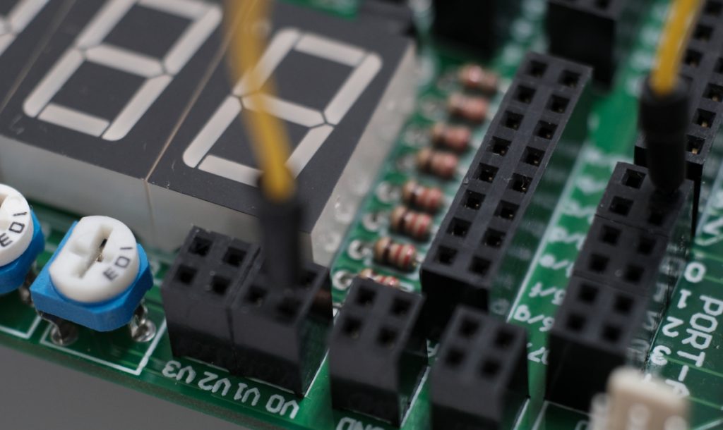
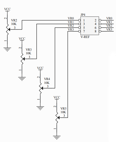
The circuit diagram of the adjustable resistor is shown in Figure 6 and the resulting example is shown in Video 1.
from PCK-1000
#pragma config OSC = HS
#pragma config OSCS = ON
#pragma config PWRT = OFF
#pragma config BOR = ON
#pragma config BORV = 25
#pragma config WDT = OFF
#pragma config WDTPS = 128
#pragma config STVR = ON
#pragma config LVP = ON
#pragma config CP0 = OFF
#pragma config CP1 = OFF
#pragma config CP2 = OFF
#pragma config CP3 = OFF
#pragma config CPB = OFF
#pragma config CPD = OFF
#pragma config WRT0 = OFF
#pragma config WRT1 = OFF
#pragma config WRT2 = OFF
#pragma config WRT3 = OFF
#pragma config WRTC = OFF
#pragma config WRTB = OFF
#pragma config WRTD = OFF
#pragma config EBTR0 = OFF
#pragma config EBTR1 = OFF
#pragma config EBTR2 = OFF
#pragma config EBTR3 = OFF
#pragma config EBTRB = OFF

#define _XTAL_FREQ 20000000

#include <xc.h>

void setup() {
    TRISA = 0b00000001; // AN0
    TRISD = 0x00; // input
    ADCON0 = 0B00000001;             // ADC Configurations bits - ADC on
    ADCON1 = 0B10001110;             // AN0 as AD, Internal REF V
}

unsigned int result;

void loop() {
    __delay_us(10);
    ADCON0bits.GO = 1;
    while (ADCON0bits.GO_nDONE); // wait
    result = ((ADRESH<<8)|ADRESL);
    if (result<113) {
        PORTD = 0b00000000;
    }
    else if (result < 226) {
        PORTD = 0b00000001;
    }
    else if (result < 339) {
        PORTD = 0b00000011;
    }
    else if (result < 452) {
        PORTD = 0b00000111;
    }
    else if (result < 565) {
        PORTD = 0b00001111;
    }
    else if (result < 678) {
        PORTD = 0b00011111;
    }
    else if (result < 791) {
        PORTD = 0b00111111;
    }
    else if (result < 904) {
        PORTD = 0b01111111;
    }
    else {
        PORTD = 0b11111111;
    }
}

void main(void) {
    setup();
    while (1) {
        loop();
    }
    return;
}
Conclusion
From this article, the reader has learned the working principle of ADC as well as how to control the operation of the analog to digital signal converter module of the PIC18F458 microcontroller that connects AN0 or pin RA0 to V0 on the test board. And display the results at the 8 LED tubes connected to PORTD, it will be found that reading the value from the analog signal is not difficult. But setting the PCFG is important for the operation of the converter sector inside the microcontroller chip, and it is important to set the ADON to 1 and set the channel number to match the selected pin to enable the functionality of the chosen pin. Finally, have fun with programming.
(C) 2022, By Anuchart Boonmark, Jarut Busarathid and Danai Jedsadathitikul
Updated 2022-03-27