In the previous article, we introduced the boards used in computer architecture labs and the software used in practice. This time, we will discuss the features and diagrams inside the PIC18F458 from Microchip‘s documentation as a basis for programming the capabilities of the microcontroller in the next article (The details of the PIC16F877 can be read from this article.).
Microcontroller Features
PIC18F458 is a high-performance microcontroller and has a higher amount of Flash memory than other chips in the 8-bit family as detailed below.
RISC processor
- Program memory can have a maximum size of 2 MB.
- Storage memory can have a maximum volume of 4KB.
- Runs up to 10 MIPS or 10 million instructions per second.
- Supports clock signals up to 40MHz by using a 4MHz to 10MHz transmitter as input through a PLL (Pulse Lock Loop) circuit.
- The instruction set is 16 bits in size and can refer to 8 bits of data location.
- Support for interrupts with many levels, can be set the priority.
- There is a multiplication cycle of 8 bits of data, multiplied by 8 bits of data in a single cycle.
Peripheral device connection feature
- Current sink to 25mA
- Current Source to 25mA
- It has 3 pins for supporting external interrupts.
- The Timer0 module works as an 8/16-bit counter or timer, with a prescaler set to 8-bit resolution.
- Timer1 and Timer3 modules work as 16-bit counters or timers.
- The Timer2 module works as an 8-bit timer or counter with an 8-bit register and is used as the main body of PWM (Pulse Width Modulate).
- Supports the use of the second clock generator for Timer1 and Timer3 separately from the main clock generator sent to the microcontroller.
- There is a CCP module (Capture/Compare/PWM) for capturing the signal, comparing the signal and sending a pulse with desire width.
- Input detection is 16-bit, it takes 6.25ns to run.
- Comparison can compare 16-bit signals with speed of 100ns.
- The PWM signal output is defined as a resolution of 1 to 10 bits, with 8 bits operating at 156kHz and 10 bits at approximately 39kHz.
- Supports motor control by outputting 1, 2 or 4 PWM signals at the same time.
- Can define the polarity of the PWM
- Set the PWM termination time.
- Supports 3-wire SPI and I2C in Master and Slave modes.
- Operate USART as an interrupt.
Working with analog signals
- There is an analog-to-digital signal converter circuit or ADC (Analog-to-Digital) with a resolution of converting to 10 bits for 8 channels and supports conversion both in power-saving mode and can be used simultaneously with all 8 pins.
- There is a programmable analog comparator module for multiplexing.
- There is a reference voltage determination module.
- There is a low voltage detection module in interrupt mode.
- Can command to reset itself when LVD occurs, also known as Brown-out Reset (BOR).
CAN Bus
Special Features of Microcontrollers
- Supports self-resetting when DC voltage is supplied to the chip or POR (Power-on-Reset).
- Support to set the working time after the occurrence of POR or BOR called the Power-up Timer (PWRT).
- Supports the default timing of the clock provider to reset itself until the clock signal stabilizes, known as Oscillator Start-up Timer (OST).
- There is a WDT (Watchdog timer) for a timer to reset itself if the written program does not report back in a specified period. To prevent problems with the program malfunction, which may affect the performance of the system.
- Can protect the program code in the chip.
- There is a power saving mode.
- Support PPL
- Supports the use of a second clock signal with a frequency of 32 kHz.
- Self-programmable via ICSP (In-Circuit Serial Programming) with 2 pins.
Flash memory technology
- Use energy-saving high-speed flash memory.
- Work at voltage 2.0-5.5V
- Supports working in the industry standard temperature range.
The features of the PIC18F458 can be summarized as follows.
- Program Memory
- Flash : 32KB
- Number of instructions that can be stored : 16384
- Data memory
- SRAM: 1536 bytes
- EEPROM : 256 bytes
- I/O: 33 pins
- ADC : 8 pins
- Number of input pins for signal comparator circuit work: 2 pins
- CCP/ECPP (PWM): 1/1
- MSSP
- Supports SPI
- Supports I2C
- Supports USART
- Timer
- 1 8-bit
- 3 16-bit
The arrangement of the pins of the PDIP chassis of the PIC18F458 microcontroller in Figure 1 is as shown in Figure 2.
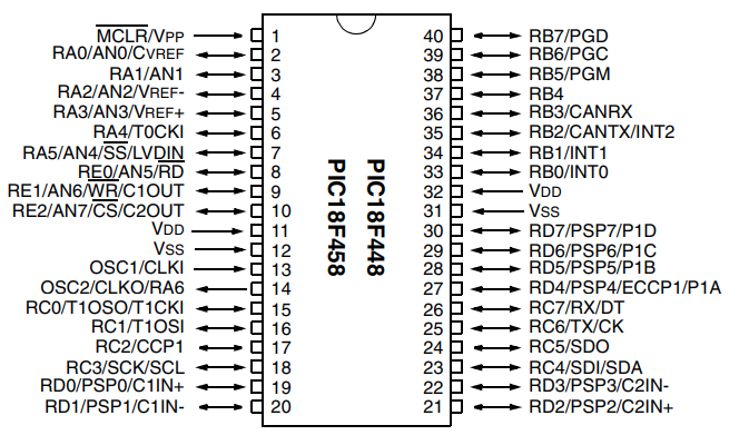
From : p.4 of PIC18F458 Datasheet
From Figures 2 and 3, it can be seen that the PIC18F458 microcontroller has 40 pins of the chassis, divided into pins for power input (VDD/VSS), clock pins (OSC1/OSC2), and pins for connecting to ports for different duty.
Working parts
Within a microcontroller, it is often the combination of multiple functions under a single chip. Likewise, the PIC18F458 microcontroller has internal components as shown in Figure 3.
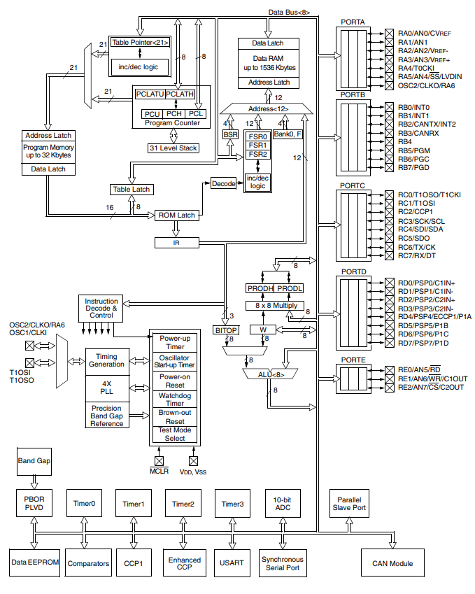
From : p.11, Figure 1-2: PIC18F448/458 Block Diagram
From Figure 3, it can be seen that the internal operation of the chip consists of various circuit parts according to the properties mentioned at the beginning of the article. And when considered in detail, you will see how the relationship of each part is connected where the arrowheads of the lines indicate the direction of receiving/sending data of each section. Therefore, we would like to refer to the summary as follows:
- The Data Bus is an 8-bit data bus based on the chip architecture and is compatible with all modules within the chip that transmit/receive data between them.
- The size of the Address Bus or the position reference bus is 21 bits.
- The transmitted data has both 8-bit and 16-bit (refer to Data Latch).
- Ports used are as follows.
- PORTA has RA0, RA1, RA2, RA3, RA4, RA5, OSC2
- PORTB has RB0, RB1, RB2, RB3, RB4, RB5, RB6, RB7
- PORTC has RC0, RC1, RC2, RC3, RC4, RC5, RC6, RC7
- PORTD has RD0, RD1, RD2, RD3, RD4, RD5, RD6, RD7
- PORTE has RE0, RE1, RE2
- The processing of the ALU unit is performed in 8-bit and has 8×8 data sectors or 8 bits multiplied by 8 bits in a single operation.
In the sector for connecting the OSC or clock signal to the microcontroller, the crystal and capacitor must be connected according to the circuit in Figure 4 and the tables in Figures 5 and 6.

From p.19, Figure 2-1 Crystal/Ceramic Resonator Operation (HS, XT, LP or LP OSC Configuration)
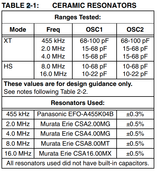
From p.19, Table 2-1: Ceramic Resonators
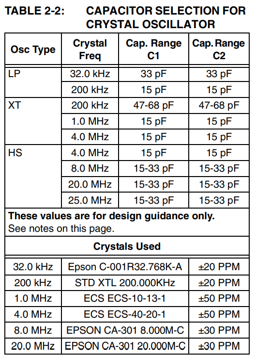
From p.20, Table 2-2: Capacitor Selection for Crystal Oscillatow
The IC uses a clock signal by looking at the nature of the cycle, which states that 1 instruction consists of 1-2 cycles, each cycle is divided into 4 parts: Q1, Q2, Q3 and Q4. Hence, the overall speed of PIC is equal to the clock frequency divided by 4. But the PIC18F458 model has a PLL circuit, it can accelerate the clock signal to a maximum of 4 times, using the same crystal frequency as the lower-generation PIC microcontrollers, but it can be accelerated up to 4 times faster or vice versa, meaning that this family of chips operates 1 cycle within 1 clock (except for jump commands and jump comparison).
Connecting to use the same image from the PIC16F877 that has been used as shown in Figure 7 means that with 1 microcontroller, power supply, crystal, resistor, capacitor and switch as shown in Figure 7, this chip can be used.
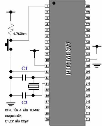
From article : Guide to PIC16F877 ] Ep.2 … architecture of PIC16F877 and 16F84 ….
Conclusion
From this article, the reader has learned in more detail the different parts of the PIC18F458 microcontroller. And will find that the work of this family of chips has a speed of 1 instruction per clock signal, which is a high speed. It also has a 10-bit ADC module and a PWM that can be configured to run simultaneously on either 2 or 4 pins, allowing both 2 and 4 motors to run simultaneously, reducing the latency of the motor. The actuation of each pin at a time makes the operation more accurate. And more importantly, we hope that the understanding of the parts or knowing the functions of the parts from this article will be the basis for programming the commands. We will continue to discuss the different parts of this microcontroller in the following articles. Finally, have fun with programming.
(C) 2022, Anuchart boonmark, Jarut Busarathid and Danai Jedsadathitikul
Updated 2022-03-14