From the previous article, we have experimented with controlling the digital signal output by driving the LED circuit connected to the STM32 microcontroller board, both Cortex-M0, Cortex-M3 and Cortex-M4. to import digital signals and use an example of connecting a switch circuit to control the on or off of an LED lamp as shown in Figure 1.
Setting commands
Since the previous article, we have been using GPIO to command the LED to turn on and off, which needs to be set to enable the pin in the function MX_GPIO_Init() that is programmed STM32CubeIDE/STM32CubeMX created to provide a set of instructions for manipulating the GPIO as a set or write more code. The command to enable GPIO is
HAL_GPIO_Init( ports, &var )
The commands to enable clock-to-port binding are as follows.
__HAL_RCC_GPIOF_CLK_ENABLE()
__HAL_RCC_GPIOA_CLK_ENABLE()
Assign the functions of the GPIO.
The procedure for defining pin functions is
- Enable the use of GPIO groups.
- Set the desired pin to the default state.
- Create a type variable GPIO_InitTypeDef to use for storing settings
- Assign settings to Pin, Mide and Pull or Speed properties to variables in step 1.
- Run the setup command with the variables configured in step 2.
The command code will come out as follows
  __HAL_RCC_groupGPIO_CLK_ENABLE();

  HAL_GPIO_WritePin( GPIO, pin, GPIO_PIN_RESET );

  GPIO_InitTypeDef GPIO_InitStruct = {0};

  GPIO_InitStruct.Pin = pin;
  GPIO_InitStruct.Mode = pin_mode;
  GPIO_InitStruct.Pull = pullup_state;
  GPIO.InitStruct.Spedd = speed;
  HAL_GPIO_Init( groupGPIO, &GPIO_InitStruct );
Digital readout command
To read digital data from the input pin, the pin must be configured as GPIO_Input in the step of setting the pin and use the following commands for importing digital signals.
value = HAL_GPIO_ReadPin( GPIO, pin )
Example Code
Test circuit connection
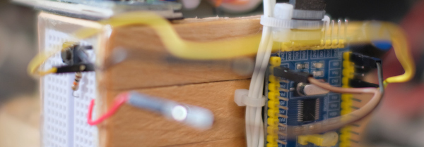
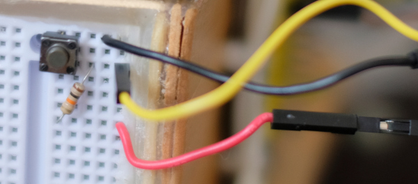
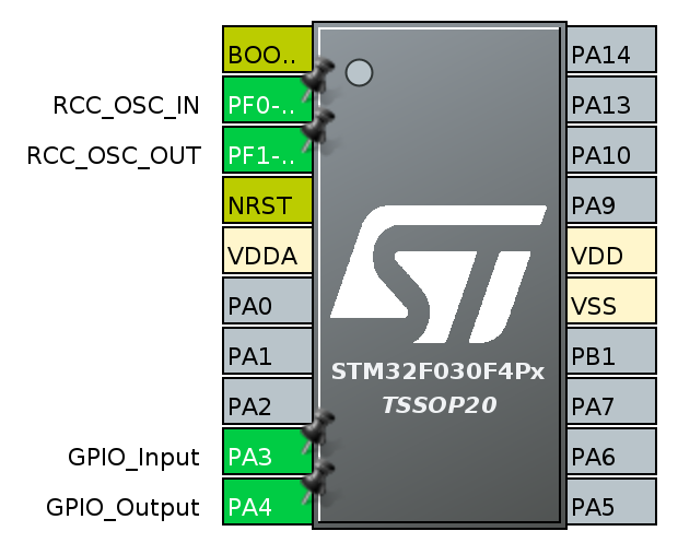
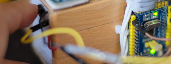
An example program for testing digital signal input from the pin of the STM32 microcontroller board is shown in Figures 2 and 3 by connecting the signal input pin (Yellow wire from picture 2) to PA3 of STM32F030F4P6 (Figure 3).
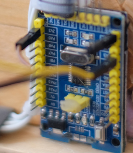
STM32F030F4P6
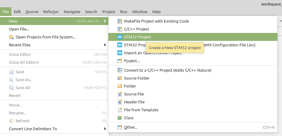
After completing the circuits in Figures 2 and 3, the next step is programming. By starting from creating a project like STM32 Project as shown in Figure 4 and then setting the working pin by setting PA4 to be GPIO_Output and PA3 to be GPIO_Input as shown in Figure 5.
When handling the pin and clock settings, get the files generated by the STM32CubeMX program and edit main.c in the main function as follows.
#include "main.h"

void SystemClock_Config(void);
static void MX_GPIO_Init(void);

int main(void)
{
  HAL_Init();
  SystemClock_Config();
  MX_GPIO_Init();
  int pa3Value=0;
  while (1)
  {
	  pa3Value = HAL_GPIO_ReadPin( GPIOA, GPIO_PIN_3 );
	  HAL_GPIO_WritePin(GPIOA, GPIO_PIN_4, pa3Value);
  }
}

void SystemClock_Config(void)
{
  RCC_OscInitTypeDef RCC_OscInitStruct = {0};
  RCC_ClkInitTypeDef RCC_ClkInitStruct = {0};

  RCC_OscInitStruct.OscillatorType = RCC_OSCILLATORTYPE_HSE;
  RCC_OscInitStruct.HSEState = RCC_HSE_ON;
  RCC_OscInitStruct.PLL.PLLState = RCC_PLL_ON;
  RCC_OscInitStruct.PLL.PLLSource = RCC_PLLSOURCE_HSE;
  RCC_OscInitStruct.PLL.PLLMUL = RCC_PLL_MUL6;
  RCC_OscInitStruct.PLL.PREDIV = RCC_PREDIV_DIV1;

  if (HAL_RCC_OscConfig(&RCC_OscInitStruct) != HAL_OK)
  {
    Error_Handler();
  }

  RCC_ClkInitStruct.ClockType = RCC_CLOCKTYPE_HCLK|RCC_CLOCKTYPE_SYSCLK
                              |RCC_CLOCKTYPE_PCLK1;
  RCC_ClkInitStruct.SYSCLKSource = RCC_SYSCLKSOURCE_PLLCLK;
  RCC_ClkInitStruct.AHBCLKDivider = RCC_SYSCLK_DIV1;
  RCC_ClkInitStruct.APB1CLKDivider = RCC_HCLK_DIV1;

  if (HAL_RCC_ClockConfig(&RCC_ClkInitStruct, FLASH_LATENCY_1) != HAL_OK)
  {
    Error_Handler();
  }
}

static void MX_GPIO_Init(void)
{
  GPIO_InitTypeDef GPIO_InitStruct = {0};

  /* GPIO Ports Clock Enable */
  __HAL_RCC_GPIOF_CLK_ENABLE();
  __HAL_RCC_GPIOA_CLK_ENABLE();

  /*Configure GPIO pin Output Level */
  HAL_GPIO_WritePin(GPIOA, GPIO_PIN_4, GPIO_PIN_RESET);

  /*Configure GPIO pin : PA3 */
  GPIO_InitStruct.Pin = GPIO_PIN_3;
  GPIO_InitStruct.Mode = GPIO_MODE_INPUT;
  GPIO_InitStruct.Pull = GPIO_NOPULL;
  HAL_GPIO_Init(GPIOA, &GPIO_InitStruct);

  /*Configure GPIO pin : PA4 */
  GPIO_InitStruct.Pin = GPIO_PIN_4;
  GPIO_InitStruct.Mode = GPIO_MODE_OUTPUT_PP;
  GPIO_InitStruct.Pull = GPIO_NOPULL;
  GPIO_InitStruct.Speed = GPIO_SPEED_FREQ_LOW;
  HAL_GPIO_Init(GPIOA, &GPIO_InitStruct);

}

void Error_Handler(void)
{
  __disable_irq();
  while (1)
  {
  }
}
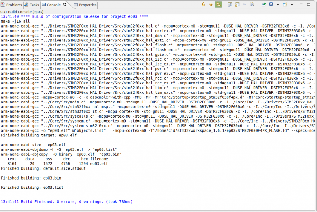
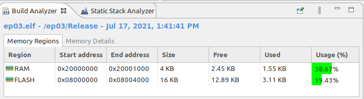
After that, set the compile to Release (described in the previous article), and compile will get the output shown in Figures 6 and 7.
Result
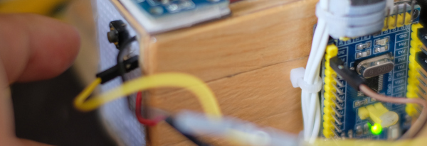
Finally, upload the program to the microcontroller and when changing the mode to work mode, the working result will be as shown in Figure 8, i.e. if you don’t press the switch, the LED that is connected to PA4 will turn off and when you press the switch, the LED will light up as shown in Figure 9.
สำหรับบอร์ดคอนโทรลเลอร์ Cortex-M3 และ Cortex-M4 ให้เลือกขาที่เป็นขา GPIO_Output และ GPIO_Input หลังจากนั้นเปลี่ยนแปลงชื่อขาและกลุ่มของขาให้ถูกต้องการทำงานจะเหมือนกันกับการใช้ Cortex-M0
Conclusion
From this article, it can be said that Programming with Cortex-M0/M3 or M4 has the same operating principle. But in each model of microcontroller, there are internal circuits that are distributed more or less equally. In summary, the program development process consists of
- Create a project for the microcontroller that you want to use.
- Define the roles and duties of the pins as follows:
- Pin for connecting with clock generating circuit.
- Define the signal output pin.
- Determine the signal input pin.
- Input digital signal.
- Input analog signal.
- Set the clock signal.
- Let the program generate the prototype instruction code.
- Modify the program to perform the required tasks.
- Complie
- Upload to board.
- Test run, if it fails, review the settings in steps 2 and 3 or review the program and compile. Upload and retest
Therefore, in this series of articles, the part of collaborative programming is discussed and will separate special uses into case studies articles. Finally, have fun with programming.
If you want to talk with us, feel free to leave comments below!!
(C) 2020-2021, By Jarut Busarathid and Danai Jedsadathitikul
Updated 2021-11-01