From the previous article, we have tried writing a program to study the elements of various files that we need, we found that there are quite a lot of details and steps. But it is an important basis for those who want to seriously and usefully study Cortex-M0 programming via STM32F030F4P6 (Figure 1), Cortex-M3 with STM32F103C (Figure 32) and Cortex-M4 with STM32F401CCU6 (Figure 27) to study of programming structure with programming tool STM32CubeIDE (Figure 2), which is the main tool used in this series of articles. This is because it combines ST’s complete development kit for ARM, including CubeMX for chip design, compiler toolkit, ST-Link program debugging tool and code editor in one tool, plus it supports both Windows, Linux and macOS operating systems.


Creating project
From Figure 2, select item “Create a New STM32 project” as shown in Figure 3 or go to File menu, select New, and select STM32 Project. The system will connect to the Internet to download data for selecting a microcontroller for use in the project as follows in Figure 4.


From Figure 4, in the Part Number field, enter STM32F030F4 to display the details of the chip. Select a chip then click the Next>> button to create a project as shown in Figure 5.

From Figure 5, give the project a name. (we named it helloSTM32Core0), define the project repository, select the language (C is selected), set the destination binary type to Executable and select the project as STM32Cube.

From the screen in Figure 6, select the desired firmware version. In this case, select V1.11.2 and save the downloaded file in the given location. When finished, click on the Finish button. The system will download the relevant file according to the steps in Figures 7 and 8. After that, the file will be created according to the structure in Figure 9 after the clock frequency configuration steps in the next section.


Setting up the pins
When everything is done, the function of the chip’s pin will be set as shown in Figure 10, or if you want to modify it, go to the Project Explorer section and double-click the ioc file extension.

The next step is to assign the functions to the pins of the microcontroller, which are divided into 3 pins: a pin for inputting an external clock signal from the 8MHz crystal on the board, a pin for defines duty for a clock signal pin to crystal and PA4 for GPIO_Output, which is the pin that connects to the LED on the STM32F030F4P6 board.
In Figure 11, click on the PF0 pin, after which a list of functions of the pin will appear. By selecting it as RCC_OSC_IN or in case of wanting to cancel, click on the item Reset_State. The result after selecting RCC_OSC_IN is as shown in Figure 12.

From Figure 12, select PF1 to set the function as RCC_OSC_OUT, the result will be as shown in Figure 13.

From Figure 13, click on pin PA4, then set the function as GPIO_Output.

If the correct duty is set, the chip’s screen will be displayed as shown in Figure 14.

Setting the clock signal
Because the board has an external crystal make it possible to create a frequency by multiplying 6 (Option X6) and select PLLCLK to enable css and will get the working frequency to 48MHz as shown in Figure 16 by clicking on the Clock Configuration tab as shown in Figure 15.


When finished, save it with the button as shown in Figure 17 or go to the File menu, select Save All. The firmware file will be downloaded and the original file is created to use as shown in Figure 18 and the result is a list of files as shown in Figure 19.


Files of program
Once the file has been created, the command can be written in the main.c file located in the Core/Src folder as shown in Figure 19.

When double-clicking on the file main.c in Figure 19, a window for editing the code as shown in Figures 20 and 21 will appear. Figure 20 shows the pin assignments from the pin assignments screen from the previous section. The GPIOF (for connecting external crystals) and GPIOA are enabled, where pin PA4 is part of GPIO group A and pin 4 or GPIO_PIN_4 has the status of GPIO_PIN_RESET or value 0. To send 1, enter number 1 or use GPIO_PIN_SET.
The GPIO_InitStruct determines the function of the pin. It can be seen that GPIO_PIN_4 is set to GPIO_MODE_OUTPUT_PP, pull-up is not used and the speed is GPIO_SPEED_FREQ_LOW. After that, configure the settings for the microcontroller according to the instructions HAL_GPIO_Init( ) as shown in Figure 19.(Figure. 20 MX_FPIO_Init())

In Figure 21, the main() function shows that a comment has been created for the programmer to read, understand and specify the location of the code in quite a detail. The main idea of the main() procedure is that HAL_Init( ) is called, after which, called SystemClock_Config() then configures the GPIO value according to the MX_GPIO_Init() function. Finally, there is an infinite loop section with while (1) { } for writing the required code like in the loop( ) function of Arduino.

The command for sending status 0 or 1 to pin PA4 called GPIO_PIN_4, which is connected to the LED circuit on the board, has the following usage patterns. Where the status is 1 or 0, or use the constants GPIO_PIN_SET and GPIO_PIN_RESET instead of numbers, while the port is the name of the active pin group. Therefore, use the port name GPIOA.
HAL_GPIO_WritePin( port, pin, state )
In the case of multi-pin commands, you can use the | sign, for example, if you want to send bit 1 to PA2, PA3 and PA4, write as follows:
HAL_GPIO_WritePin( GPIOA, GPIO_PIN_2 | GPIO_PIN_3 | GPIO_PIN_4, GPIO_PIN_SET );The command for delay in milliseconds is
HAL_Delay( millisec )
The code of main.c is as follows:
#include "main.h"

/* Private function prototypes -----------------------------------------------*/
void SystemClock_Config(void);
static void MX_GPIO_Init(void);

int main(void)
{
  /* Reset of all peripherals, Initializes the Flash interface and the Systick. */
  HAL_Init();
  /* Configure the system clock */
  SystemClock_Config();
  /* Initialize all configured peripherals */
  MX_GPIO_Init();
    /* USER CODE BEGIN WHILE */
  while (1)
  {
	  HAL_GPIO_WritePin(GPIOA, GPIO_PIN_4, 0);
	  HAL_Delay( 500 );
	  HAL_GPIO_WritePin(GPIOA, GPIO_PIN_4, 1);
	  HAL_Delay( 500 );
  }
}

void SystemClock_Config(void)
{
  RCC_OscInitTypeDef RCC_OscInitStruct = {0};
  RCC_ClkInitTypeDef RCC_ClkInitStruct = {0};

  /** Initializes the RCC Oscillators according to the specified parameters
  * in the RCC_OscInitTypeDef structure.
  */
  RCC_OscInitStruct.OscillatorType = RCC_OSCILLATORTYPE_HSE;
  RCC_OscInitStruct.HSEState = RCC_HSE_ON;
  RCC_OscInitStruct.PLL.PLLState = RCC_PLL_ON;
  RCC_OscInitStruct.PLL.PLLSource = RCC_PLLSOURCE_HSE;
  RCC_OscInitStruct.PLL.PLLMUL = RCC_PLL_MUL6;
  RCC_OscInitStruct.PLL.PREDIV = RCC_PREDIV_DIV1;
  if (HAL_RCC_OscConfig(&RCC_OscInitStruct) != HAL_OK)
  {
    Error_Handler();
  }
  /** Initializes the CPU, AHB and APB buses clocks
  */
  RCC_ClkInitStruct.ClockType = RCC_CLOCKTYPE_HCLK|RCC_CLOCKTYPE_SYSCLK
                              |RCC_CLOCKTYPE_PCLK1;
  RCC_ClkInitStruct.SYSCLKSource = RCC_SYSCLKSOURCE_PLLCLK;
  RCC_ClkInitStruct.AHBCLKDivider = RCC_SYSCLK_DIV1;
  RCC_ClkInitStruct.APB1CLKDivider = RCC_HCLK_DIV1;

  if (HAL_RCC_ClockConfig(&RCC_ClkInitStruct, FLASH_LATENCY_1) != HAL_OK)
  {
    Error_Handler();
  }
}

static void MX_GPIO_Init(void)
{
  GPIO_InitTypeDef GPIO_InitStruct = {0};

  /* GPIO Ports Clock Enable */
  __HAL_RCC_GPIOF_CLK_ENABLE();
  __HAL_RCC_GPIOA_CLK_ENABLE();

  /*Configure GPIO pin Output Level */
  HAL_GPIO_WritePin(GPIOA, GPIO_PIN_4, GPIO_PIN_RESET);

  /*Configure GPIO pin : PA4 */
  GPIO_InitStruct.Pin = GPIO_PIN_4;
  GPIO_InitStruct.Mode = GPIO_MODE_OUTPUT_PP;
  GPIO_InitStruct.Pull = GPIO_NOPULL;
  GPIO_InitStruct.Speed = GPIO_SPEED_FREQ_LOW;
  HAL_GPIO_Init(GPIOA, &GPIO_InitStruct);

}

void Error_Handler(void)
{
  __disable_irq();
  while (1)  {  }
}
Complie
When finished writing the code in main.c, select the type of project that you want to create as Release by clicking the button as shown in Figure 22 and you will see a window as shown in Figure 23. Select Configuration as Release and click the Set Active button, the Status value named Active will change from the address after Debug to the row of Release, finally, click OK to agree with the settings.


Once set to Release is complete. (Do not choose Debug to reduce the amount of code and we do not have a tool for debugging the program as well), click on the icon in Figure 24 and wait for the compilation. If there are no errors, the result will be displayed in the Console box as shown in Figure 25.


When successfully compiled, Release folder will appear in Project Explorer as shown in Figure 26.

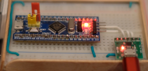
When helloSTM32Core0.bin or helloSTM32Core0.elf is obtained, use the program STM32CubeProgrammer according to the previous article, upload to the chip. After that, change the mode on the board and reset to run the program, you will find that the LED lamp on the board is switched off.
STM32F401CCU6
In the case of using Cortex-M4 chip STM32F401CCU6 or Black Pill in Figure 27, which has external crystal connectors at pins PC14 and PC15 and set the maximum speed of work to 84MHz, it has the same project construction process as Cortex-M0, but Select the type of microcontroller as shown in Figure 28.


Pins assignment
Set the functions of pins PC13, PC14 and pc15 to GPIO_Output, RCC_OSC32_ON and RCC_OSC32_OUT respectively as shown in Figure 29. To select pins PC14 and PC15, go to System Core and click RCC channel, and set High Speed Clock (HSE) and Low Speed Clock (LSE) are Crystal/Ceramic Resonator. When these 2 values are set, pins PH0, PH1, PC14 and PC15 are selected.
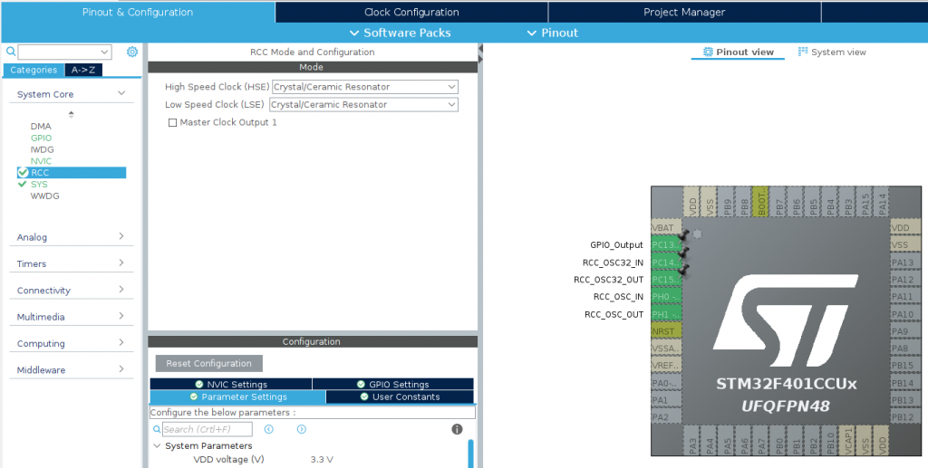
Clock setting
After defining the functions of the pins, determine the function of the clock signal. Set as shown in Figure 30 by selecting HSE on, setting /M to /25, multiplying *N to X168 and dividing /P to /2, and selecting PLLCLK, setting AHB Prescaler to /1, will get HCLK as 84MHz.

main.c
/* USER CODE BEGIN Header */
/**
******************************************************************************
* @file : main.c
* @brief : Main program body
******************************************************************************
* @attention
*
* <h2><center>© Copyright (c) 2021 STMicroelectronics.
* All rights reserved.</center></h2>
*
* This software component is licensed by ST under BSD 3-Clause license,
* the "License"; You may not use this file except in compliance with the
* License. You may obtain a copy of the License at:
* opensource.org/licenses/BSD-3-Clause
*
******************************************************************************
*/
/* USER CODE END Header */
/* Includes ------------------------------------------------------------------*/
#include "main.h"
/* Private includes ----------------------------------------------------------*/
/* USER CODE BEGIN Includes */
/* USER CODE END Includes */
/* Private typedef -----------------------------------------------------------*/
/* USER CODE BEGIN PTD */
/* USER CODE END PTD */
/* Private define ------------------------------------------------------------*/
/* USER CODE BEGIN PD */
/* USER CODE END PD */
/* Private macro -------------------------------------------------------------*/
/* USER CODE BEGIN PM */
/* USER CODE END PM */
/* Private variables ---------------------------------------------------------*/
/* USER CODE BEGIN PV */
/* USER CODE END PV */
/* Private function prototypes -----------------------------------------------*/
void SystemClock_Config(void);
static void MX_GPIO_Init(void);
/* USER CODE BEGIN PFP */
/* USER CODE END PFP */
/* Private user code ---------------------------------------------------------*/
/* USER CODE BEGIN 0 */
/* USER CODE END 0 */
/**
* @brief The application entry point.
* @retval int
*/
int main(void)
{
/* USER CODE BEGIN 1 */
/* USER CODE END 1 */
/* MCU Configuration--------------------------------------------------------*/
/* Reset of all peripherals, Initializes the Flash interface and the Systick. */
HAL_Init();
/* USER CODE BEGIN Init */
/* USER CODE END Init */
/* Configure the system clock */
SystemClock_Config();
/* USER CODE BEGIN SysInit */
/* USER CODE END SysInit */
/* Initialize all configured peripherals */
MX_GPIO_Init();
/* USER CODE BEGIN 2 */
/* USER CODE END 2 */
/* Infinite loop */
/* USER CODE BEGIN WHILE */
while (1)
{
/* USER CODE END WHILE */
HAL_GPIO_WritePin(GPIOC, GPIO_PIN_13, 0);
HAL_Delay( 500 );
HAL_GPIO_WritePin(GPIOC, GPIO_PIN_13, 1);
HAL_Delay( 500 );
/* USER CODE BEGIN 3 */
}
/* USER CODE END 3 */
}
/**
* @brief System Clock Configuration
* @retval None
*/
void SystemClock_Config(void)
{
RCC_OscInitTypeDef RCC_OscInitStruct = {0};
RCC_ClkInitTypeDef RCC_ClkInitStruct = {0};
/** Configure the main internal regulator output voltage
*/
__HAL_RCC_PWR_CLK_ENABLE();
__HAL_PWR_VOLTAGESCALING_CONFIG(PWR_REGULATOR_VOLTAGE_SCALE2);
/** Initializes the RCC Oscillators according to the specified parameters
* in the RCC_OscInitTypeDef structure.
*/
RCC_OscInitStruct.OscillatorType = RCC_OSCILLATORTYPE_HSE;
RCC_OscInitStruct.HSEState = RCC_HSE_ON;
RCC_OscInitStruct.PLL.PLLState = RCC_PLL_ON;
RCC_OscInitStruct.PLL.PLLSource = RCC_PLLSOURCE_HSE;
RCC_OscInitStruct.PLL.PLLM = 25;
RCC_OscInitStruct.PLL.PLLN = 168;
RCC_OscInitStruct.PLL.PLLP = RCC_PLLP_DIV2;
RCC_OscInitStruct.PLL.PLLQ = 4;
if (HAL_RCC_OscConfig(&RCC_OscInitStruct) != HAL_OK)
{
Error_Handler();
}
/** Initializes the CPU, AHB and APB buses clocks
*/
RCC_ClkInitStruct.ClockType = RCC_CLOCKTYPE_HCLK|RCC_CLOCKTYPE_SYSCLK
|RCC_CLOCKTYPE_PCLK1|RCC_CLOCKTYPE_PCLK2;
RCC_ClkInitStruct.SYSCLKSource = RCC_SYSCLKSOURCE_PLLCLK;
RCC_ClkInitStruct.AHBCLKDivider = RCC_SYSCLK_DIV1;
RCC_ClkInitStruct.APB1CLKDivider = RCC_HCLK_DIV2;
RCC_ClkInitStruct.APB2CLKDivider = RCC_HCLK_DIV1;
if (HAL_RCC_ClockConfig(&RCC_ClkInitStruct, FLASH_LATENCY_2) != HAL_OK)
{
Error_Handler();
}
}
/**
* @brief GPIO Initialization Function
* @param None
* @retval None
*/
static void MX_GPIO_Init(void)
{
GPIO_InitTypeDef GPIO_InitStruct = {0};
/* GPIO Ports Clock Enable */
__HAL_RCC_GPIOC_CLK_ENABLE();
__HAL_RCC_GPIOH_CLK_ENABLE();
/*Configure GPIO pin Output Level */
HAL_GPIO_WritePin(GPIOC, GPIO_PIN_13, GPIO_PIN_RESET);
/*Configure GPIO pin : PC13 */
GPIO_InitStruct.Pin = GPIO_PIN_13;
GPIO_InitStruct.Mode = GPIO_MODE_OUTPUT_PP;
GPIO_InitStruct.Pull = GPIO_NOPULL;
GPIO_InitStruct.Speed = GPIO_SPEED_FREQ_LOW;
HAL_GPIO_Init(GPIOC, &GPIO_InitStruct);
}
/* USER CODE BEGIN 4 */
/* USER CODE END 4 */
/**
* @brief This function is executed in case of error occurrence.
* @retval None
*/
void Error_Handler(void)
{
/* USER CODE BEGIN Error_Handler_Debug */
/* User can add his own implementation to report the HAL error return state */
__disable_irq();
while (1)
{
}
/* USER CODE END Error_Handler_Debug */
}
#ifdef USE_FULL_ASSERT
/**
* @brief Reports the name of the source file and the source line number
* where the assert_param error has occurred.
* @param file: pointer to the source file name
* @param line: assert_param error line source number
* @retval None
*/
void assert_failed(uint8_t *file, uint32_t line)
{
/* USER CODE BEGIN 6 */
/* User can add his own implementation to report the file name and line number,
ex: printf("Wrong parameters value: file %s on line %d\r\n", file, line) */
/* USER CODE END 6 */
}
#endif /* USE_FULL_ASSERT */
/************************ (C) COPYRIGHT STMicroelectronics *****END OF FILE****/
Program compilation
From the code when compiling the program without any errors, it will be shown in Figure 31. After receiving the file, upload it to the chip with the program STM32CubeProgrammer to test. If there is no fault, the LED connected to the PC13 pin will turn off alternately every 250msec.

STM32F103C8
For Cortex-M3, which uses a microcontroller STM32F103C8 or Blue Pill as shown in Figure 32, the pin structure is the same as the Black Pill board.
To create a project, select the chip as STM32F103C8 as shown in Figure 33. After that, set the project name as shown in Figure 34 and install the firmware as shown in Figure 35 respectively.


In the step of assigning the functions of the pin, select the pin as shown in Figure 36 and in the step of setting the clock signal as shown in Figure 37, after that, Save All to generate the prototype code.


From the prototype code, edit main.c as follows. After selecting compile as Release and compile, it will report the result of memory usage as shown in Figure 36 and the result of compilation as shown in Figure 37.
/* USER CODE BEGIN Header */
/**
******************************************************************************
* @file : main.c
* @brief : Main program body
******************************************************************************
* @attention
*
* <h2><center>© Copyright (c) 2021 STMicroelectronics.
* All rights reserved.</center></h2>
*
* This software component is licensed by ST under BSD 3-Clause license,
* the "License"; You may not use this file except in compliance with the
* License. You may obtain a copy of the License at:
* opensource.org/licenses/BSD-3-Clause
*
******************************************************************************
*/
/* USER CODE END Header */
/* Includes ------------------------------------------------------------------*/
#include "main.h"
/* Private includes ----------------------------------------------------------*/
/* USER CODE BEGIN Includes */
/* USER CODE END Includes */
/* Private typedef -----------------------------------------------------------*/
/* USER CODE BEGIN PTD */
/* USER CODE END PTD */
/* Private define ------------------------------------------------------------*/
/* USER CODE BEGIN PD */
/* USER CODE END PD */
/* Private macro -------------------------------------------------------------*/
/* USER CODE BEGIN PM */
/* USER CODE END PM */
/* Private variables ---------------------------------------------------------*/
/* USER CODE BEGIN PV */
/* USER CODE END PV */
/* Private function prototypes -----------------------------------------------*/
void SystemClock_Config(void);
static void MX_GPIO_Init(void);
/* USER CODE BEGIN PFP */
/* USER CODE END PFP */
/* Private user code ---------------------------------------------------------*/
/* USER CODE BEGIN 0 */
/* USER CODE END 0 */
/**
* @brief The application entry point.
* @retval int
*/
int main(void)
{
/* USER CODE BEGIN 1 */
/* USER CODE END 1 */
/* MCU Configuration--------------------------------------------------------*/
/* Reset of all peripherals, Initializes the Flash interface and the Systick. */
HAL_Init();
/* USER CODE BEGIN Init */
/* USER CODE END Init */
/* Configure the system clock */
SystemClock_Config();
/* USER CODE BEGIN SysInit */
/* USER CODE END SysInit */
/* Initialize all configured peripherals */
MX_GPIO_Init();
/* USER CODE BEGIN 2 */
/* USER CODE END 2 */
/* Infinite loop */
/* USER CODE BEGIN WHILE */
while (1)
{
/* USER CODE END WHILE */
HAL_GPIO_WritePin(GPIOC, GPIO_PIN_13, 0);
HAL_Delay( 500 );
HAL_GPIO_WritePin(GPIOC, GPIO_PIN_13, 1);
HAL_Delay( 500 );
/* USER CODE BEGIN 3 */
}
/* USER CODE END 3 */
}
/**
* @brief System Clock Configuration
* @retval None
*/
void SystemClock_Config(void)
{
RCC_OscInitTypeDef RCC_OscInitStruct = {0};
RCC_ClkInitTypeDef RCC_ClkInitStruct = {0};
/** Initializes the RCC Oscillators according to the specified parameters
* in the RCC_OscInitTypeDef structure.
*/
RCC_OscInitStruct.OscillatorType = RCC_OSCILLATORTYPE_HSE;
RCC_OscInitStruct.HSEState = RCC_HSE_ON;
RCC_OscInitStruct.HSEPredivValue = RCC_HSE_PREDIV_DIV1;
RCC_OscInitStruct.HSIState = RCC_HSI_ON;
RCC_OscInitStruct.PLL.PLLState = RCC_PLL_ON;
RCC_OscInitStruct.PLL.PLLSource = RCC_PLLSOURCE_HSE;
RCC_OscInitStruct.PLL.PLLMUL = RCC_PLL_MUL9;
if (HAL_RCC_OscConfig(&RCC_OscInitStruct) != HAL_OK)
{
Error_Handler();
}
/** Initializes the CPU, AHB and APB buses clocks
*/
RCC_ClkInitStruct.ClockType = RCC_CLOCKTYPE_HCLK|RCC_CLOCKTYPE_SYSCLK
|RCC_CLOCKTYPE_PCLK1|RCC_CLOCKTYPE_PCLK2;
RCC_ClkInitStruct.SYSCLKSource = RCC_SYSCLKSOURCE_PLLCLK;
RCC_ClkInitStruct.AHBCLKDivider = RCC_SYSCLK_DIV1;
RCC_ClkInitStruct.APB1CLKDivider = RCC_HCLK_DIV2;
RCC_ClkInitStruct.APB2CLKDivider = RCC_HCLK_DIV1;
if (HAL_RCC_ClockConfig(&RCC_ClkInitStruct, FLASH_LATENCY_2) != HAL_OK)
{
Error_Handler();
}
}
/**
* @brief GPIO Initialization Function
* @param None
* @retval None
*/
static void MX_GPIO_Init(void)
{
GPIO_InitTypeDef GPIO_InitStruct = {0};
/* GPIO Ports Clock Enable */
__HAL_RCC_GPIOC_CLK_ENABLE();
__HAL_RCC_GPIOD_CLK_ENABLE();
/*Configure GPIO pin Output Level */
HAL_GPIO_WritePin(GPIOC, GPIO_PIN_13, GPIO_PIN_RESET);
/*Configure GPIO pin : PC13 */
GPIO_InitStruct.Pin = GPIO_PIN_13;
GPIO_InitStruct.Mode = GPIO_MODE_OUTPUT_PP;
GPIO_InitStruct.Pull = GPIO_NOPULL;
GPIO_InitStruct.Speed = GPIO_SPEED_FREQ_LOW;
HAL_GPIO_Init(GPIOC, &GPIO_InitStruct);
}
/* USER CODE BEGIN 4 */
/* USER CODE END 4 */
/**
* @brief This function is executed in case of error occurrence.
* @retval None
*/
void Error_Handler(void)
{
/* USER CODE BEGIN Error_Handler_Debug */
/* User can add his own implementation to report the HAL error return state */
__disable_irq();
while (1)
{
}
/* USER CODE END Error_Handler_Debug */
}
#ifdef USE_FULL_ASSERT
/**
* @brief Reports the name of the source file and the source line number
* where the assert_param error has occurred.
* @param file: pointer to the source file name
* @param line: assert_param error line source number
* @retval None
*/
void assert_failed(uint8_t *file, uint32_t line)
{
/* USER CODE BEGIN 6 */
/* User can add his own implementation to report the file name and line number,
ex: printf("Wrong parameters value: file %s on line %d\r\n", file, line) */
/* USER CODE END 6 */
}
#endif /* USE_FULL_ASSERT */
/************************ (C) COPYRIGHT STMicroelectronics *****END OF FILE****/


When uploading ep02f103.bin to the chip and changing the mode to work mode, the result will be as shown in Figures 38 and 39.


Conclusion
From this article, you will find that STM32 programming tools are available from project creation. Determination of pin functions, Clock setting, code editing, compiling, and uploading to the board. This helps a lot to hide the writing parts from the original article. However, if readers understand the previous article, they can get a better overview of programming code management. And can edit the interrupt table or the beginning of the program from the top to the lower level of programming. As for the article in part 2, the reader has gone through the process of using the tool and learned to configure the GPIO pin configuration and time delay. Finally, have fun with programming.
If you want to talk with us, feel free to leave comment below!!
(C) 2020-2021, By Jarut Busarathid and Danai Jedsadathitikul
Updated 2021-10-27